


Tel Number
181-3719-5600
Chemical vapor deposition (CVD) coating system is an experimental equipment widely used in fields such as materials science, semiconductor manufacturing, optics, and electronic engineering. Through CVD technology, various thin film materials can be deposited on the substrate surface, which have the advantages of controllable composition, high purity, and strong adhesion. Let’s take a detailed look at what experiments can be done with CVD coating systems below!
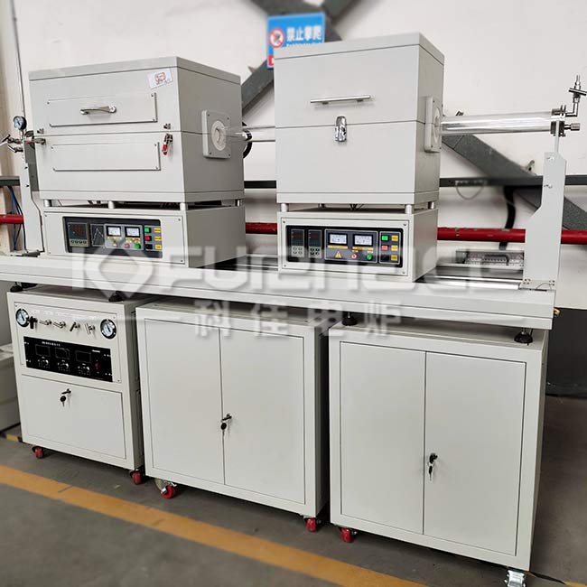
Customized dual furnace slide CVD furnace (click on the image to view product details)
1. Preparation of semiconductor thin films
Deposition of silicon-based thin films: such as polycrystalline silicon and amorphous silicon thin films, used for solar cells, thin film transistors (TFTs), etc.
Silicon nitride (Si ∝ N ₄) thin film: used as an insulation layer or passivation layer in integrated circuits and microelectromechanical systems (MEMS).
Silicon carbide (SiC) thin film: used for high-temperature and high-frequency electronic devices.
2. Deposition of oxide thin films
Silicon dioxide (SiO ₂) thin film: widely used as a gate oxide layer or insulating layer in semiconductor devices.
Aluminum oxide (Al ₂ O3) thin film: used for high dielectric constant (High-k) materials to enhance device performance.
Zinc oxide (ZnO) thin film: It has transparent and conductive properties and can be used in solar cells, sensors, etc.
3. Deposition of nitride thin films
Titanium nitride (TiN) film: used as a diffusion barrier or conductive layer for integrated circuit interconnects.
Aluminum nitride (AlN) thin film: used for piezoelectric sensors and surface acoustic wave devices (SAW).
4. Deposition of carbon based thin films
Diamond like carbon (DLC) film: With high hardness and low friction coefficient, it is used as a wear-resistant coating for mechanical parts.
Graphene thin film: Large area, high-quality graphene is prepared by CVD method and applied in electronic devices, sensors, etc.
5. Deposition of Composite Thin Films
Multilayer thin film structure: such as metal insulator semiconductor (MIS) structure, used for microelectronic devices.
Nanocomposite thin film: Preparation of nanostructured thin films with special functions by controlling deposition conditions.
6. Deposition of functional thin films
Photocatalytic thin film: such as titanium dioxide (TiO ₂) thin film, used for photocatalytic decomposition of water or pollutants.
Magnetic thin films: such as iron, cobalt, nickel and their alloy thin films, used for magnetic storage devices.
Superconducting thin film: such as yttrium barium copper oxide (YBCO) thin film, used for high-temperature superconducting devices.
7. Surface modification experiment
Improving the hardness, wear resistance, or corrosion resistance of the substrate material: Surface modification of metal or ceramic substrates by depositing hard coatings (such as TiN, DLC).
Improving optical performance: such as depositing anti reflective coatings to increase the transmittance of optical components.
8. Exploration of new materials
Two dimensional materials, such as hexagonal boron nitride (h-BN), transition metal sulfides (TMDs), etc., were prepared by CVD method and their physical and chemical properties were studied.
Topological insulators, such as bismuth antimony tellurium (Bi ₂ Se ∝), are used to study novel quantum effects.
9. Process parameter optimization experiment
Study the influence of deposition temperature, gas flow rate, pressure and other parameters on film quality: By controlling variables, optimize the deposition process to obtain the best film performance.
Research on the growth mechanism of thin films: Study the growth kinetics of thin films through in-situ monitoring techniques such as spectroscopic ellipsometry and reflection high-energy electron diffraction (RHEED).
10 Device Preparation and Performance Testing
Prepare complete device structures such as thin film transistors (TFTs), solar cells, sensors, etc., and conduct electrical and optical performance tests.
Reliability testing: Study the stability of thin films in high temperature, high humidity and other environments.
11. Environment and Energy Applications
Catalytic materials: Deposition of thin films with high catalytic activity for environmental remediation or energy conversion (such as water electrolysis, fuel cells).
Gas sensor: Deposition of thin films sensitive to specific gases for environmental monitoring.
Experimental precautions
Safety: Toxic or flammable gases (such as silane and hydrogen) may be used during the CVD process, and safety operating procedures must be strictly followed.
Equipment maintenance: Regularly clean the reaction chamber, replace vulnerable parts, and ensure sedimentation quality.
Substrate treatment: The surface cleanliness and pretreatment of the substrate are important for the quality of the film.
Overall, chemical vapor deposition (CVD) electric furnaces have a wide range of applications in the laboratory. Before choosing, it is important to communicate with relevant technical personnel about the desired technical parameters in order to purchase a CVD coating system that is suitable for your own experiment!Click to learn more CVD devices! Or click on online customer service to learn more about product information!
Contact Information
E-mail: