


Tel Number
181-3719-5600
Plasma enhanced chemical vapor deposition (PECVD) technology is a process that rapidly undergoes chemical reactions at lower temperatures, utilizing plasma energy to chemically react gaseous or vapor state chemicals in a reactor to form solid deposits at the gas phase or gas-solid interface. It activates chemical reactions by introducing plasma into the reaction chamber, utilizing the energy of the plasma to quickly deposit the required thin film at lower temperatures.
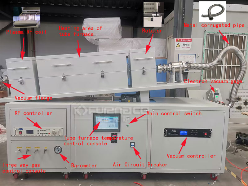
PECVD detailed analysis diagram (click on the image to view the product details)
PECVD (Plasma Enhanced Chemical Vapor Deposition) is a common thin film deposition technique widely used in the preparation of thin film materials, such as silicon oxides, silicon nitride, etc.
1.The process of PECVD:
① Substrate preparation: Surface cleaning and treatment are key steps in the PECVD process. The substrate is usually a silicon wafer or other material suitable for thin film deposition.
② Pre treatment: Before the substrate is exposed to the plasma environment in a vacuum chamber, it is usually necessary to undergo pre-treatment, such as exposure to hydrogen or oxygen atmospheres.
③ Gas phase precursor supply: Gas phase precursors are precursor gases used for thin film growth, such as dimethyl ether, dimethyl methane, ammonia, etc. These gases are introduced into the vacuum chamber.
④ Plasma excitation: By adding electrical energy or radio frequency field, gas is ionized in a vacuum chamber to form plasma. This plasma excites the gas-phase precursor, causing it to decompose into active ions and free radicals.
⑤ Sedimentation layer generation: Active gas-phase substances react with the substrate surface to form the required thin film deposition layer.
⑥ Control and monitoring: Accurate control and monitoring of temperature, gas flow rate, pressure and other parameters are required during the process to ensure the quality and uniformity of the film.
2.The main application areas of PECVD are:
① Semiconductor manufacturing: used to prepare thin films such as silicon oxides and silicon nitride, for the manufacturing of semiconductor devices such as transistors and integrated circuits.
② Flat panel display: used for preparing transparent conductive films, zinc oxide films, etc., widely used in the production of liquid crystal displays (LCDs) and organic light-emitting diodes (OLEDs).
③ Solar cells: used for depositing thin film materials, such as amorphous silicon and silicon nitride, for the preparation of solar cells.
④ Optical coating: used for preparing reflective films, anti reflective films, etc., applied to coatings of optical components.
⑤ Protective coating: used to prepare protective films, such as scratch resistant, waterproof, and anti-corrosion coatings.
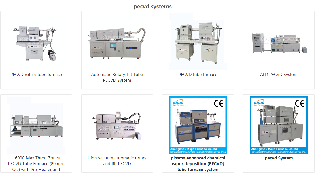
Various types of PECVD (click on the image to view more PECVD classifications)
3. Advantages of PECVD:
① High controllability: The PECVD process has high controllability and can achieve precise control of film properties by adjusting process parameters.
② Uniformity: PECVD can uniformly deposit thin films on large-area substrates, ensuring that the prepared films have consistent performance.
③ Low temperature deposition: Compared to other thin film preparation techniques, PECVD is usually carried out at relatively low temperatures, which is beneficial for the application of temperature sensitive materials.
④ High speed growth: PECVD has a relatively high growth rate and is suitable for large-scale production.
4、 Precautions when using PECVD:
① Substrate surface treatment: The treatment of the substrate surface is crucial for the quality and adhesion of the film, and requires careful treatment before deposition.
② Selection of gas-phase precursors: Different gas-phase precursors determine the properties of deposited films, and selecting the appropriate gas-phase precursor is crucial for the functionality of the film.
③ Complex equipment: PECVD systems are usually complex and require professional operation and maintenance.
5、 PECVD Summary:
Compared with traditional CVD technology, PECVD technology has higher deposition rate and lower temperature requirements, making it widely used in fields such as microelectronics, optoelectronics, and solar energy.
In addition, PECVD technology can be used to deposit various thin film materials, such as silicon-based films, nitride films, carbide films, etc., and the composition and properties of the films can also be controlled by adjusting reaction parameters. Click to learn more about PECVD products, or click to consult online customer service for more product solutions!
Contact Information
E-mail: