


Tel Number
181-3719-5600
CVD tube furnace coating has multiple advantages and is widely used in material preparation and surface modification. Let’s take a detailed look below!
Advantage
High coating quality and good uniformity: CVD tube furnace can achieve uniform deposition of reaction gas on the substrate surface by precisely controlling reaction conditions such as temperature, pressure, gas flow rate, etc., forming a uniform and dense thin film. For example, in the preparation of semiconductor thin films, a uniform thin film helps to improve the performance and stability of the device.
High purity: Coating is carried out in a vacuum or specific atmosphere environment, reducing the influence of impurities on the film and obtaining high-purity film materials. This is essential for industries that require extremely high purity, such as microelectronics and optoelectronics.
Strong adhesion: During the CVD coating process, a strong chemical bond is formed between the film and the substrate through a chemical reaction, which gives the film good adhesion and is not easily peeled off.
Wide applicability
Rich material types: can deposit thin films of various materials, including metals, oxides, nitrides, carbides, etc. For example, silicon-based thin films can be deposited for solar cells, thin-film transistors (TFTs), etc; Deposition of silicon nitride thin films as insulation or passivation layers, applied in integrated circuits and microelectromechanical systems (MEMS); Deposition of silicon carbide thin films for high-temperature and high-frequency electronic devices.
Diverse substrate shapes: For substrates with complex shapes, CVD tube furnaces can also achieve good coating effects. This is because the coating process is based on gas-phase reactions, and the reaction gases can diffuse and react uniformly on the substrate surface.
High process flexibility
Strong parameter adjustability: By adjusting parameters such as reaction temperature, pressure, gas type and flow rate, reaction time, etc., the composition, structure, and properties of the film can be precisely controlled. For example, in the preparation of alumina thin films, materials with different dielectric constants can be obtained by changing the reaction conditions to meet the needs of different devices.
Multi layer and composite thin films can be prepared: thin films of different materials can be sequentially deposited according to design requirements to prepare multi-layer thin film structures or nano composite thin films, thereby endowing the films with special properties and functions. The metal insulator semiconductor (MIS) structure is used in microelectronic devices, and nanocomposite films can obtain nanostructures with special functions by controlling deposition conditions.
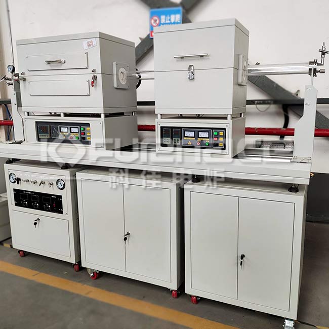
Customized dual body CVD electric furnace (click on the image to view product details)
Summarize
CVD tube furnace has a wide range of applications in coating, with obvious advantages. It is necessary to communicate the requirements with relevant technical personnel before choosing, so as to customize a CVD tube furnace that is more suitable for oneself!Click to learn more CVD devices! Or click on online customer service to learn more about product information!
Contact Information
E-mail: