


Tel Number
181-3719-5600
Plasma enhanced chemical vapor deposition (PECVD) electric furnace, as a commonly used thin film preparation equipment, achieves low-temperature deposition by exciting gas molecules with plasma, demonstrating advantages in multiple fields. Let’s take a detailed look at the application scope of plasma PECVD electric furnaces below!
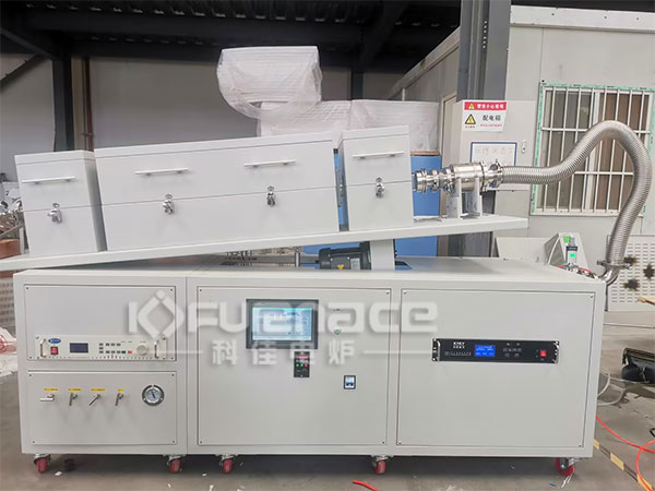
Commonly used tubular PECVD electric furnace (click on the image to view product details)
1. Semiconductor and Microelectronics Field
Thin film deposition
Silicon nitride (SiNx): used for passivation layers, anti reflection layers, and insulation layers in chips. PECVD can achieve high-density deposition at low temperatures (<400 ℃), avoiding damage to devices caused by high temperatures. Silicon oxide (SiO ₂): As a gate insulating layer or interlayer dielectric, PECVD deposited thin films have low pinhole density and good interface characteristics. Polycrystalline silicon (poly Si): used for the channel layer of thin film transistors (TFTs), PECVD can control grain size and doping concentration. advantage Low temperature process compatible with flexible substrates (such as polyimide), suitable for wearable devices. The film thickness uniformity is high (within ± 2%), meeting the process requirements.
2. Photovoltaic industry
Surface passivation of solar cells
Hydrogenated silicon nitride (SiNx: H): Thin films deposited by PECVD have a high hydrogen content (>10%), which can effectively passivate silicon surface defects and improve battery conversion efficiency (>25%).
Aluminum oxide (Al ₂ O3): As a back passivation layer, PECVD can achieve atomic layer deposition (ALD) level control and reduce composite losses.
Heterojunction Battery (HJT)
PECVD simultaneously deposits intrinsic amorphous silicon (i-a-Si: H) and doped layers, simplifying the process flow and reducing production costs.
3. Display and Lighting Technology
Organic Light Emitting Diodes (OLEDs)
Encapsulation layer: The water oxygen permeability (WVTR) of SiNx/SiO ₂ stacked thin films deposited by PECVD is less than 10 ⁻⁶ g/m ² · day, which extends the device life.
Buffer layer: used between flexible OLED substrate and functional layer to relieve stress and improve adhesion.
Micro LED display
Prepare passivation layer and insulation layer to solve the sidewall damage problem of micro LED after massive transfer.
4. Optics and Sensor Field
Optical thin film
Anti reflective film/anti reflective film: TiO ₂/SiO ₂ multilayer films deposited by PECVD can achieve high transmittance (>99%) in specific wavelength bands (such as visible light).
Filter: Used in spectral analyzers to achieve narrowband filtering by precisely controlling the thickness of the thin film.
sensor
Gas sensor: Deposition of sensitive materials such as SnO ₂ to improve the detection sensitivity of CO and NOx.
Biosensor: SiO ₂/TiO ₂ composite film prepared by PECVD is used to immobilize biomolecules and enhance signal response.
5. Energy storage and conversion
Lithium Ion Battery
Solid state electrolyte: LiPON thin films deposited by PECVD have an ion conductivity>10 ⁻⁶ S/cm and are used for all solid state batteries.
Electrode protective layer: Deposition of Al ₂ O3 on the surface of lithium metal negative electrode to inhibit lithium dendrite growth.
fuel cell
Proton exchange membrane (PEM): The surface of Nafion membrane is modified by PECVD to improve proton conductivity and durability.
6. Biomedical and Flexible Electronics
Biocompatible coating
Deposition of diamond-like carbon (DLC) or SiC thin films to reduce the inflammatory response of implantable devices.
flexible sensor
Deposition of piezoelectric materials (such as ZnO) on polymer substrates for wearable health monitoring.
Summary of Technical Advantages
Low temperature process: reduces thermal budget, compatible with flexible substrates and temperature sensitive materials.
High deposition rate: Compared to traditional CVD, the rate is increased by more than 10 times, making it suitable for large-scale production.
Controllable film quality: precise control of film composition and structure by adjusting plasma parameters (power, pressure, gas ratio).
Summarize
Plasma PECVD electric furnace has become a core technology equipment in semiconductor, photovoltaic, display and other fields due to its low temperature, high efficiency and controllable characteristics. With the advancement of materials science and plasma physics, its application scope will further expand to cutting-edge fields such as quantum computing and neural morphology chips.Click to learn more PECVD devices! Or click on online customer service to learn more about product information!
Contact Information
E-mail: