


Tel Number
181-3719-5600
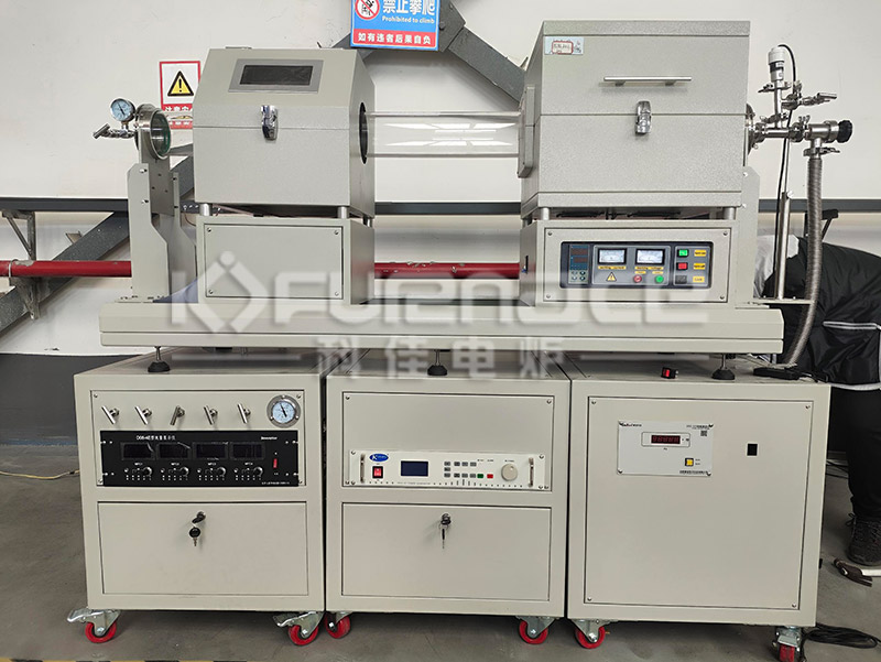
The laboratory uses chemical vapor deposition (PECVD) electric furnace as a commonly used equipment for material preparation, which can carry out various experiments covering fields such as thin film deposition, nanomaterial preparation, device manufacturing, material modification, and cutting-edge research. Let’s take a detailed look below!
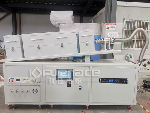
PECVD slide furnace commonly used for graphene growth (click on the image to view product details)
1. Thin film deposition experiment: core functions and diversified applications
PECVD electric furnace can achieve high-quality thin film preparation under low temperature conditions through plasma enhanced chemical vapor deposition technology, and is widely used in fields such as electronics, optics, and energy.
Semiconductor thin film deposition
Silicon based thin film: Deposition of polycrystalline silicon and amorphous silicon thin films, used for solar cells, thin film transistors (TFTs), etc. For example, in solar cells, adjusting plasma parameters to control the refractive quality of optical coatings can improve the photoelectric conversion efficiency.
Dielectric layer thin film: Preparation of thin films such as silicon dioxide (SiO ₂) and silicon nitride (Si ∝ N ₄) as gate oxide or insulation layers, applied in integrated circuits and microelectromechanical systems (MEMS).
High dielectric constant material: Deposition of aluminum oxide (Al ₂ O3) thin film to enhance device performance.
Functional thin film deposition
Transparent conductive film: Preparation of zinc oxide (ZnO) film for use in solar cells, sensors, etc.
Diffusion barrier layer: Deposition of titanium nitride (TiN) thin film, applied to integrated circuit interconnects.
Piezoelectric and Surface Acoustic Wave Devices: Preparation of Aluminum Nitride (AlN) Thin Films for Piezoelectric Sensors and Surface Acoustic Wave Devices (SAW).
Wear resistant coating: Deposition of diamond-like carbon (DLC) film to improve the hardness and wear resistance of mechanical parts.
New material film
Graphene thin film: Large area, high-quality graphene is prepared by PECVD method and applied in electronic devices and sensors.
Two dimensional materials: Synthesize two-dimensional materials such as hexagonal boron nitride (h-BN) and transition metal sulfides (TMDs), and study their physical and chemical properties.
Topological insulators: Preparation of bismuth antimony tellurium (Bi ₂ Se ∝) and other topological insulators to explore novel quantum effects.
2. Nanomaterial Preparation Experiment: Controllable Synthesis of Morphology and Size
By adjusting reaction conditions (such as temperature, gas flow rate, plasma power) and substrate materials, PECVD electric furnaces can synthesize nanomaterials with different morphologies and sizes, meeting the needs of fields such as nanoelectronics and nanomedicine.
Nanoparticles and nanowires: Synthesize metal or semiconductor nanoparticles and nanowires for use in nanoelectronic devices and photocatalytic reactions.
Nanocomposite thin film: Control deposition conditions to prepare nanostructured thin films with special functions, such as photocatalytic thin films (such as titanium dioxide TiO ₂ thin films, used for decomposing water or pollutants).
3. Device Manufacturing Experiment: A Bridge from Laboratory to Industrialization
PECVD electric furnace supports the preparation and testing of complete device structures, promoting the commercialization of laboratory achievements.
Microelectronic devices: Prepare thin film transistors (TFTs), solar cells, sensors, etc., and conduct electrical and optical performance tests.
Magnetic storage devices: Deposition of thin films of iron, cobalt, nickel, and their alloys for the manufacture of magnetic storage devices.
High temperature superconducting devices: Preparation of yttrium barium copper oxygen (YBCO) thin films for application in high-temperature superconducting devices.
4. Material modification experiment: the main technology for improving material properties
By depositing hard coatings or functional films, PECVD electric furnaces can greatly improve the performance of substrate materials.
Surface hardening and wear resistance improvement: Deposition of hard coatings such as TiN and DLC for surface modification of metal or ceramic substrates.
Optical performance optimization: Deposition of anti reflective coating to improve the transmittance of optical components.
Biocompatibility modification: Preparation of biocompatible thin film materials for use in medical fields such as cardiovascular disease treatment.
5. Frontier Research Experiment: Exploring New Boundaries in Materials Science
PECVD electric furnace provides an experimental platform for cutting-edge research in materials science, promoting theoretical innovation and technological breakthroughs.
Research on the growth mechanism of thin films: Study the growth kinetics of thin films through in-situ monitoring techniques such as spectroscopic ellipsometry and reflection high-energy electron diffraction.
Process parameter optimization: Study the influence of deposition temperature, gas flow rate, pressure and other parameters on film quality, and optimize the deposition process.
Reliability testing: Study the stability of thin films in high temperature, high humidity and other environments, and evaluate their long-term performance.
6. High temperature and atmosphere control experiment: meeting diverse process requirements
As an experimental equipment, PECVD electric furnace supports various research experiments such as high-temperature atmosphere sintering, atmosphere reduction, vacuum annealing, etc., providing strong support for research in the fields of materials science and engineering.
Ceramic sintering: used for powder roasting and sintering of ceramic materials to prepare high-performance ceramic products.
Powder metallurgy: The formation of metal or ceramic materials through gas-phase reactions provides a new preparation method for the field of powder metallurgy.
Preparation of gas sensors: Deposition of thin films sensitive to specific gases for environmental monitoring.
Overall, there are numerous experimental fields for chemical vapor deposition (PECVD) electric furnaces. Before choosing, you can communicate with relevant technical personnel about the experimental parameters you want, so as to customize a PECVD electric furnace that is more suitable for your experimental needs!Click to learn more PECVD devices! Or click on online customer service to learn more about product information!
Contact Information
E-mail: