


Tel Number
181-3719-5600
The experimental electric furnace for plasma vapor deposition (PECVD) coating combines plasma technology and vapor deposition process, demonstrating significant advantages in material surface modification, thin film preparation, and other fields. Let’s take a detailed look at the advantages of PECVD experimental electric furnace below!
The experimental electric furnace for plasma vapor deposition (PECVD) coating combines plasma technology and vapor deposition process, demonstrating significant advantages in material surface modification, thin film preparation, and other fields. Let’s take a detailed look at the advantages of PECVD experimental electric furnace below!
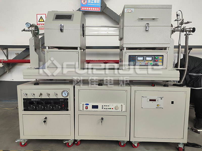
Slide PECVD tube furnace (click on the picture to view product details)
1. Low temperature deposition to protect the substrate material
principle
PECVD uses radio frequency power to excite gas ionization and form plasma, utilizing high-energy particles (such as ions and electrons) in the plasma to promote chemical reactions, rather than relying solely on high-temperature thermal decomposition. This characteristic allows the sedimentation process to be completed at lower temperatures (usually 200-500 ℃).
advantage
Protect thermal sensitive substrates: Suitable for substrates such as plastics and polymers that are not resistant to high temperatures, to avoid deformation or performance degradation caused by high temperatures.
Reduce energy consumption: Compared to traditional chemical vapor deposition (CVD) that requires a high temperature of over 800 ℃, PECVD greatly reduces energy consumption and lowers experimental costs.
Extended material selection: It can handle a wider range of substrate materials, including flexible electronic devices, biomedical materials, etc.
Application scenarios
Deposition of Transparent Conductive Oxide (TCO) Thin Films for Flexible Solar Cells.
Preparation of anti reflective coatings on polymer substrates.
2. High sedimentation rate, improving experimental efficiency
principle
The high-energy particles in the plasma accelerate the decomposition and reaction rate of gas molecules, while enhancing the impact on the substrate surface and promoting thin film growth.
advantage
Shorten the experimental period: The deposition rate can reach several times to tens of times that of traditional CVD, for example, the deposition time of silicon nitride film can be shortened from several hours to several tens of minutes.
Improving production capacity: In industrial production, high sedimentation rates directly translate into higher production efficiency.
Application scenarios
Rapid thin film deposition in the semiconductor industry, such as silicon nitride passivation layers.
Batch preparation of optical thin films (such as anti reflective and reflective films).
3. Excellent film quality and stable performance
principle
Plasma bombardment can eliminate pores and defects in thin films, while promoting the bonding between the film and the substrate, forming a dense and uniform coating.
advantage
High adhesion: The film has a high bonding strength with the substrate and is not easily peeled off.
Low defect density: fewer defects such as pinholes and cracks, improving the corrosion resistance and mechanical properties of the film.
Controllability: By adjusting parameters such as RF power and gas flow rate, the composition, thickness, and structure of the film can be controlled.
Application scenarios
The insulation layer or protective layer (such as silicon dioxide, silicon nitride) in microelectronic devices.
Preparation of antibacterial coatings on the surface of medical devices.
4. High process flexibility, adaptable to diverse needs
principle
PECVD can achieve thin film deposition of different materials and structures by adjusting parameters such as gas type, RF power, and pressure.
advantage
Material diversity: It can deposit various materials such as metals, semiconductors, insulators, ceramics, etc. (such as SiO ₂, Si ∝ N ₄, DLC, TiN, etc.).
Structural controllability: By changing the process conditions, thin films with different structures such as nanocrystals, amorphous, and porous can be prepared.
Composite function: capable of preparing complex structures such as gradient films and multilayer films.
Application scenarios
Multi functional coatings in optical devices, such as anti reflection and anti reflection composite films.
Preparation of efficient catalyst carrier thin films in the field of energy.
5. Environmentally friendly and energy-saving, in line with the trend of green manufacturing
principle
PECVD is carried out at low temperatures and has high gas utilization efficiency, reducing the emission of harmful gases and energy consumption.
advantage
Low pollution: The amount of exhaust gas generated during the process is minimal and can be further purified through exhaust gas treatment systems.
Resource conservation: Low gas consumption, high material utilization, and reduced experimental costs.
Compliant with environmental standards: meeting the environmental requirements in laboratories and industrial production.
Application scenarios
Preparation of thin-film solar cells in the field of green energy.
Surface coating treatment of environmentally friendly packaging materials.
6. Optimization of experimental electric furnace design to enhance operational experience
Temperature field equilibrium
Adopting good heating elements and temperature control systems to ensure temperature uniformity inside the furnace and avoid film stress problems caused by local overheating or excessive temperature gradients.
intelligent control system
Integrated fully automatic intelligent control system, supporting program heating, real-time monitoring, and fault diagnosis, simplifying operation processes, and improving experimental repeatability.
modular design
The vacuum system, gas supply system, etc. adopt modular design, which is easy to maintain and upgrade, and extends the service life of the equipment.
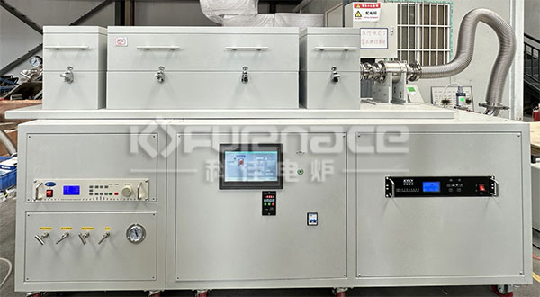
Rotating and tilting PECVD electric furnace (click on the image to view product details)
7. Typical application cases
semiconductor industry
Prepare a passivation layer on the surface of the wafer to improve device stability.
Deposition of low dielectric constant materials to reduce signal delay.
Optical field
Prepare high-precision optical thin films (such as laser interference filters).
Repair surface damage of optical components and extend their service life.
Biomedicine
Deposition of antibacterial coating on the surface of medical devices to reduce the risk of infection.
Prepare a biocompatible implant surface modification layer.Click to learn more PECVD devices! Or click on online customer service to learn more about product information!
Contact Information
E-mail: