English
 简体中文
简体中文 Français
 日本語
日本語 한국어
한국어 Português
 Русский
 Español




Tel Number
181-3719-5600
PECVD, also known as plasma enhanced chemical vapor deposition equipment, is a core industrial equipment in the field of vacuum thin film coating. It relies on plasma excitation gas to achieve low-temperature nano film deposition. With the advantages of low-temperature film formation, dense and uniform film layer, and adaptability to the vast majority of thermosensitive substrates, it firmly ranks in the commonly used list of essential process equipment in the semiconductor chip, photovoltaic solar energy, and optical components industries. Many equipment procurement and process R&D personnel are unclear about which functional film layers can be prepared by PECVD, the differences in selection in different fields, and the process value. Below, we will explain the basic working principle and core technological advantages of PECVD in a simple way. We will break down the application scenarios, coating types, and process functions in three mainstream tracks to facilitate research institutes, new material factories, and photovoltaic enterprises to select and purchase according to their needs.
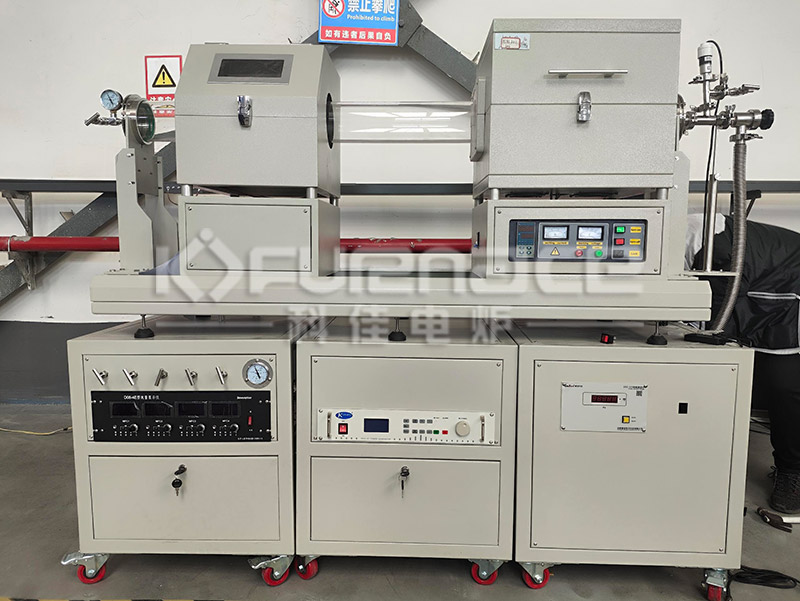
PECVD slide furnace commonly used for graphene growth (click on the image to view product details)
1. What is PECVD equipment? Basic working principle
PECVD belongs to an improved CVD chemical vapor deposition coating equipment, which is different from traditional high-temperature CVD that relies on heat driven gas reaction to deposit thin films. It introduces process gases such as silane, ammonia, and oxygen into a closed vacuum chamber, and ionizes the gas through radio frequency electric field to form low-temperature plasma; High energy electrons break down gas molecules to generate active functional groups, which undergo chemical reactions on the surfaces of substrates such as silicon wafers, glass, and optical lenses, and deposit solid functional thin films at the nanometer to micrometer level layer by layer.
Core characteristic: Low temperature sedimentation
Traditional CVD deposition of silicon nitride and silicon oxide films requires high temperatures of 650-850 ℃; PECVD can control the substrate temperature within the range of 100-400 ℃ without burning out already formed circuits, organic substrates, and flexible substrates. This is also the fundamental reason why it is widely used in the microelectronics, photovoltaic, and optical industries.
Two types of dielectric films are commonly prepared in daily mass production: silicon dioxide (SiO ₂) and silicon nitride (SiN ₓ). Special films such as silicon nitride oxide, amorphous silicon, and silicon carbide can also be prepared as needed.
2. Five core technological advantages of PECVD equipment
Strong low-temperature adaptability: can be coated on glass, plastic, flexible PI film, and wired wafers, with exclusive process solutions for thermal sensitive materials;
Controllable film accuracy: The film thickness error is small, and the refractive index, density, and stress can be adjusted by gas ratio and power;
Excellent step coverage capability: The concave and convex surfaces of chips and microstructures can be uniformly coated without voids or broken films, suitable for micro nano device manufacturing processes;
Excellent airtightness and barrier properties: Silicon nitride film is dense and impermeable to water vapor and ions, with good moisture resistance, corrosion resistance, and oxidation resistance;
High mass production efficiency: fast deposition rate, adaptable to single piece and tube batch production, balancing laboratory research and development with industrial assembly line manufacturing.
3. In depth explanation of application scenarios in the three core areas
(1) Semiconductor Microelectronics: Process Equipment Used in the Entire Chip Manufacturing Process
PECVD is a commonly used equipment for silicon-based integrated circuits, MEMS microelectromechanical systems, and LED chips from wafer manufacturing to packaging and factory delivery. It runs through the entire process of front-end manufacturing, back-end interconnection, and back-end packaging, and mature processes above 7nm cannot be separated from this process.
a. Front end wafer process application
Interlayer insulating dielectric layer (SiO ₂ silicon oxide film): Deposition of silicon dioxide film to isolate multiple layers of metal conductive lines and prevent short circuits in the internal circuits of the chip; Silicon oxide prepared using TEOS technology has better filling effect for high aspect ratio trenches;
Etching barrier layer and gate sidewall (SiN silicon nitride): Silicon nitride has high hardness and is resistant to acid and alkali etching. As a photolithography process barrier layer, it accurately defines the size of the chip microstructure;
Shallow trench isolation STI filling, active region passivation: isolates leakage between transistors, reduces chip power consumption, and improves device operation stability.
b. Backend metal interconnect process
In the copper wiring process, SiCN and silicon nitride barrier layers are deposited to prevent copper ions from diffusing into the dielectric layer, ensuring the long-term reliable operation of multi-layer interconnect structures.
c. Chip passivation protection (core use)
After the chip processing is completed, a dense silicon nitride protective film is deposited on the outermost layer of the wafer, which is like putting a waterproof and dustproof shell on the chip: isolating water vapor, sodium ion impurities, acid and alkali corrosion in the air, resisting slight mechanical scratches, and greatly extending the service life of the chip. It is the last protective process before the integrated circuit leaves the factory.
d. Extend segmentation scenarios
MEMS pressure sensors, acceleration sensors, microfluidic chips: using PECVD low-temperature characteristics to conformal coating inside micro/nano grooves, producing insulation layers, sealing layers, and sacrificial layers; The sidewall insulation of Mini/Micro LED chips and the barrier of water and oxygen in device packaging both rely on PECVD coating technology.
(2) Photovoltaic solar energy field: key core equipment for improving battery conversion efficiency
The photovoltaic industry is a track for the mass production and application of PECVD equipment. Each silicon wafer of crystalline silicon solar cells needs to go through the PECVD coating process, which directly determines the power generation efficiency and service life of the photovoltaic panel. The mainstream PERC, TOPCon, and HJT battery technology routes all rely on this equipment.
a. PERC conventional monocrystalline/polycrystalline cells (with large market stock)
Deposition of silicon nitride anti reflection passivation film (SiN ₓ: H) on the front of the silicon wafer, with two core functions:
① Optical anti reflection: The specific refractive index of silicon nitride can reduce the reflection of sunlight on the surface of silicon wafers, allowing more sunlight to enter the silicon substrate and convert electrical energy, directly improving conversion efficiency;
② Hydrogen passivation repair: The coating process releases hydrogen ions, repairs lattice defects inside the silicon wafer, reduces electronic recombination losses, and improves open circuit voltage and power generation. Simultaneously depositing silicon nitride film on the back of the battery to achieve back passivation and anti reflection.
b. TOPCon Tunnel Oxide Passivation Contact Battery
By using PECVD ultra-thin deposition of silicon dioxide tunneling layer and doped polycrystalline silicon layer, a backside passivation structure is created to reduce the recombination loss of charge carriers on the backside of silicon wafers. This is currently the mainstream process for mass production of photovoltaic cells.
c. HJT heterojunction, perovskite thin film solar cell
HJT batteries rely on PECVD low-temperature deposition of intrinsic amorphous silicon and doped silicon thin films. The silicon wafer does not withstand high temperatures throughout the process, and the silicon substrate is zero damaged, resulting in a higher open circuit voltage of the battery; Flexible perovskite photovoltaic modules rely on low-temperature PECVD to prepare window layers and buffer layers on flexible substrates, suitable for the production of flexible photovoltaic products.
Summary: The core value of photovoltaic PECVD is to reduce light reflection, passivate silicon wafer defects, increase power generation, and reduce attenuation rate.
(3) Optical Coating Field: Main Equipment for Precision Optical Component Thin Film Preparation
The optical industry utilizes PECVD to more accurately control the refractive index, transmittance, and thickness of thin films, and prepares various optical functional thin films that are suitable for the production of visible light, infrared, and laser components, meeting the dual requirements of hard wear resistance and optical transparency.
a、 Conventional optical lenses, car lenses, security camera lenses
Silicon dioxide anti reflective film: a multi-layer film based base film that enhances the transmittance of the lens and eliminates image glare and ghosting;
Silicon nitride hard protective film: The outermost coating of the lens is resistant to friction, oil stains, and moisture erosion, extending the outdoor service life of optical lenses.
b、 Optical communication devices, laser resonators, optical waveguides
Deposition of SiO ₂/SiN ₓ multilayer optical dielectric film on quartz substrate, preparation of fiber coupling devices, passive chips, and waveguide structures, precise control of optical path transmission loss, widely used in 5G optical modules and fiber sensing equipment.
c. AR/VR optical substrate, infrared window plate
Deposition of infrared anti reflective and moisture-proof composite film for infrared temperature measurement and night vision device windows; AR diffractive optical waveguide lenses rely on PECVD to prepare high-precision dielectric grating film layers, ensuring imaging clarity and lightweight requirements.
4. Comparison Table of Core Differences in PECVD Equipment Selection in Three Major Fields
| Application Fields | Common deposition films | Process temperature | Core appeal | Equipment structure selection |
| Semiconductor chip | SiO ₂, Si ∝ N ₄ SiCN | 280~350℃ | High purity of the film layer, approaching zero particle defects, and good step coverage | Single piece chamber, high-purity vacuum system |
| Photovoltaic cells | Hydrogenated silicon nitride SiN ₓ: H | 300~400℃ | Fast sedimentation rate, uniform refractive index, suitable for large-scale walking | Tube PECVD (optional for mass production) |
| Optical components | SiO ₂, SiN multilayer film system | 150~300℃ | Adjustable refractive index, high transmittance, low film stress | Small chamber, research dual-use equipment |
5. PECVD equipment is suitable for extending niche scenarios
In addition to the three mainstream tracks, it is also widely used in the fields of inorganic packaging layer for OLED flexible screens (blocking water and oxygen to prevent screen burn-in), wear-resistant protective coating for hard alloy cutting tools, biocompatible film for medical implant devices, and insulation coating for energy storage battery separators. With the advantage of low-temperature coating, it continuously expands the application boundaries of new materials.
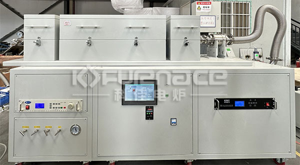
Commonly used PECVD (click on image to view product details)
6. Purchase Summary
Research and production of chips and MEMS precision microelectronics: Choose high-purity single-chip PECVD to prioritize ensuring film uniformity and cleanliness;
Photovoltaic cell mass production line: Tube type high-capacity PECVD has higher cost-effectiveness, meeting the continuous coating needs of large quantities of silicon wafers;
Optical lens and laboratory new material research and development: small desktop PECVD, flexible parameter adjustment, suitable for multi film process debugging.
Conclusion
The process parameters, cavity size, and RF power of PECVD equipment can be customized according to the coating material, substrate specifications, and production capacity requirements.Click to learn more PECVD devices! Or click on online customer service to learn more about product information!
Contact Information
E-mail: