


Tel Number
181-3719-5600
PECVD (Plasma Enhanced Chemical Vapor Deposition) has a wide and critical application in the semiconductor industry. Let’s take a detailed look below!
1. Deposition of thin film materials
Insulation layer deposition: PECVD technology can accurately deposit high-quality insulation layers, such as silicon nitride (SiN) films and silicon dioxide (SiO ₂) films. These thin films play a role in isolation and protection in semiconductor devices, with good electrical properties and chemical stability. For example, silicon nitride thin films are often used as gate dielectric layers for transistors and dielectric layers for metal interconnects to prevent impurity diffusion and improve device stability and reliability.
Passivation layer deposition: Passivation layer is used to protect semiconductor devices from external environmental erosion. PECVD technology can prepare uniform and dense passivation layers, improving the reliability and stability of devices.
Deposition of low-k dielectric materials: With the continuous advancement of semiconductor technology, the demand for low-k dielectric materials is increasing. PECVD technology can prepare dielectric materials with low dielectric constants, which helps to reduce capacitance effects between interconnects and improve device performance.
Deposition of other functional layers: PECVD technology can also be used to prepare key thin film layers in semiconductor memories, as well as to manufacture other functional layers in integrated circuits, such as anti reflective coatings, anti reflective coatings, etc. These coatings can be used to protect or enhance the optical properties of semiconductor components.
2. Optoelectronic device manufacturing
Solar cells: PECVD plays a crucial role in the preparation of solar cells. For example, depositing a silicon nitride anti reflection film on the surface of a crystalline silicon solar cell can reduce light reflection, improve the cell’s absorption efficiency of light, and thus enhance the cell’s photoelectric conversion efficiency. In addition, PECVD technology can also be used to prepare key materials such as transparent conductive films in solar panels.
LED manufacturing: In the manufacturing of LEDs, PECVD technology is used to deposit transparent conductive films and anti reflective layers to improve the luminous efficiency and stability of LEDs.
3. Manufacturing of Micro Electro Mechanical Systems (MEMS) Devices
Thin films deposited by PECVD serve as structural and sacrificial layers in MEMS devices, enabling complex microstructure design and manufacturing. For example, PECVD technology can be used to prepare structures such as micro beams and micro films with specific shapes and sizes, providing a foundation for the functional implementation of MEMS devices.
4. Production of silicon-based optoelectronic devices
PECVD technology also plays an important role in the production process of silicon-based optoelectronic devices. For example, it can be used to prepare key components such as optical waveguides and gratings, which have important application value in optoelectronic integrated circuits.
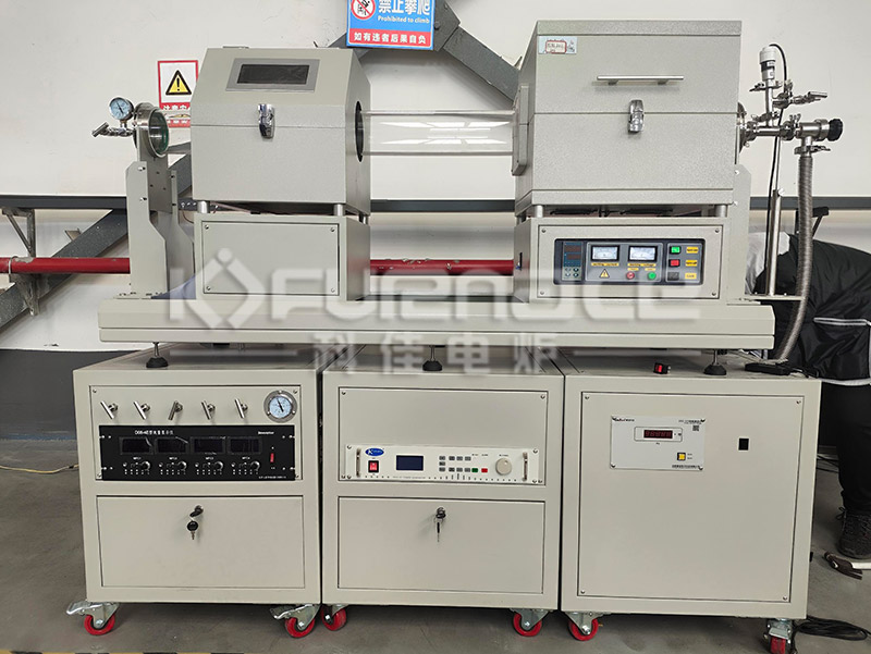
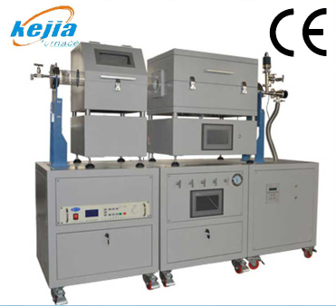
PECVD slide furnace commonly used for graphene growth (click on the image to view product details)
Overall, PECVD coating systems have a wide range of applications in the semiconductor industry. Before choosing, it is important to communicate with relevant technical personnel about the parameters you want, so that you can customize PECVD coating equipment that is more suitable for your own experiments!Click to learn more PECVD devices! Or click on online customer service to learn more about product information!
Contact Information
E-mail: