


Tel Number
181-3719-5600
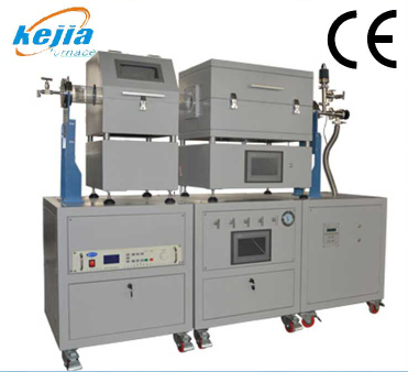
The laboratory tube PECVD electric furnace is an experimental equipment that uses plasma enhanced chemical vapor deposition (PECVD) technology for thin film deposition. Let’s take a detailed look at this type of product below!
1. Core principle
PECVD technology generates plasma through glow discharge or radio frequency excitation, which decomposes reaction gases (such as silane, ammonia, etc.) into active functional groups (such as SiH3, NH ₂, etc.) under the action of plasma. These active groups undergo chemical reactions on the surface of the sample to form solid thin films (such as silicon nitride, silicon oxide, etc.). The non-equilibrium characteristics of plasma (electron temperature much higher than gas temperature) significantly reduce the activation energy of the reaction, allowing thin film deposition to be carried out at low temperatures (usually 300-1000 ℃), avoiding damage to the substrate material caused by high temperatures.
2.Structural composition
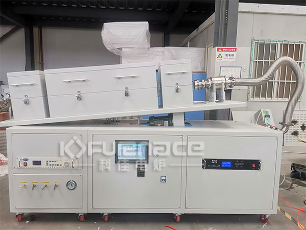
The laboratory tubular PECVD electric furnace is usually composed of the following modules:
Tube furnace body:
Using quartz or corundum tubes, high temperature resistance and strong chemical stability.
Equipped with independent temperature control zone, supporting temperature gradient control (such as single temperature zone or multi temperature zone design).
The heating element is made of resistance wire or silicon carbide rod, with a maximum temperature of 1200 ℃ and a long-term working temperature of ≤ 1100 ℃.
Temperature control accuracy ± 1 ℃, temperature uniformity ± 5 ℃, supporting multi-stage program temperature control (such as 30 time temperature curves).
Plasma generation system:
RF power supply (generates high-frequency electric field to excite gas ionization.
Matching network optimizes power transmission efficiency and reduces reflected power.
Special gas path design (such as multi-point RF feeding) ensures uniform distribution of plasma and improves film uniformity.
Vacuum and pneumatic system:
A vacuum pump (such as a rotary vane pump or molecular pump) is used to evacuate the chamber (with a maximum vacuum degree of 10 ⁻ ³ Pa).
Mass flow meters (MFCs) accurately control the flow rate of reaction gases and support the mixing of 1-6 gases.
The fast flange sealing structure ensures the airtightness of the cavity and prevents air leakage.
Safety and Control System:
Safety functions such as over temperature alarm, overcurrent protection, and disconnection prompt.
Can be equipped with a touch screen or industrial computer for human-computer interaction, supporting data recording and analysis.
3. Technical features
Low temperature deposition: Plasma activation reduces reaction temperature, suitable for temperature sensitive substrates such as plastics and flexible substrates.
High deposition rate: high concentration of active groups, fast film growth rate.
Good film quality:
Dense without pinholes, strong adhesion, and good step coverage.
Thin film stress, refractive index, and other properties can be controlled by adjusting plasma parameters such as power and pressure.
Wide material compatibility: capable of depositing oxides (SiO ₂), nitrides (Si ∝ N ₄), carbides (SiC), and binary/multicomponent compounds.
Process flexibility: Supports co deposition (such as SiON), doping (such as boron/phosphorus doped silicon), and multi-layer structure preparation.
4. Application Fields
Semiconductors and Microelectronics:
Deposition of gate oxide layer (SiO ₂), passivation layer (Si ∝ N ₄), and low-k dielectric material.
Manufacturing thin film transistors (TFTs), solar cells (such as amorphous/microcrystalline silicon cells), and MEMS devices.
Optics and Optoelectronics:
Prepare optical coatings such as anti reflective films, reflective films, and filters.
Deposition of transparent conductive oxides (such as ITO, ZnO) for touch screens LED。
Energy and Environmental Protection:
Synthesize graphene, two-dimensional materials (such as hexagonal boron nitride h-BN), and nanowires/particles.
Preparation of fuel cell electrolyte membranes, lithium-ion battery separators, and catalytic electrodes.
biomedical science:
Deposition of biocompatible coatings (such as DLC, TiN) for artificial joints and dental implants.
Preparation of drug sustained-release carrier and biosensor functional layer.
Surface engineering:
Deposition of wear-resistant coatings (such as DLC), anti-corrosion coatings (such as Al ₂ O3), and anti fouling coatings.
Surface hardening treatment of metal/ceramic substrates to enhance mechanical properties.
5. Selection suggestions
Temperature requirement: Select the maximum temperature of the furnace body (such as 1200 ℃) based on the highest experimental temperature.
Film uniformity: Prioritize equipment with multi-point RF feeding and special gas path design.
Gas control: High precision experiments require high-precision mass flow meters.
Safety and scalability: Confirm whether the equipment has over temperature alarm, in-situ monitoring, and process compatibility.
Budget and after-sales service: Choose brands with high cost-effectiveness and comprehensive after-sales service while ensuring performance.Click to learn more PECVD devices! Or click on online customer service to learn more about product information!
Contact Information
E-mail: